The aim of this project was to implement a low cost version of the clock using the existing functionality of the Simkit's CCU clock interface coupled with a 2 line by 16 character LCD display together with 3 push button switches.
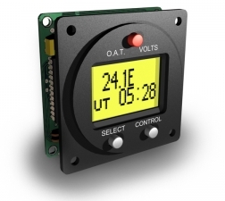
The Simkits digital clock is based on the Davtron M803 clock and is a very realistic representation.
The Simkits version is available as either a USB device or with a direct connection to the Simkits CCU (main control interface board).
The only issue with this device is the cost, approx £350 for the USB version and £300 for the CCU version.
In the case of the CCU version, the entire logic processing takes place within the CUU, the clock itself is a display and three push switches.
Another possible solution is the GSA71, manufactured by Flight Illusion. This is a again an expensive option, with the clock costing approx £250 + £100 for an interface card
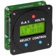
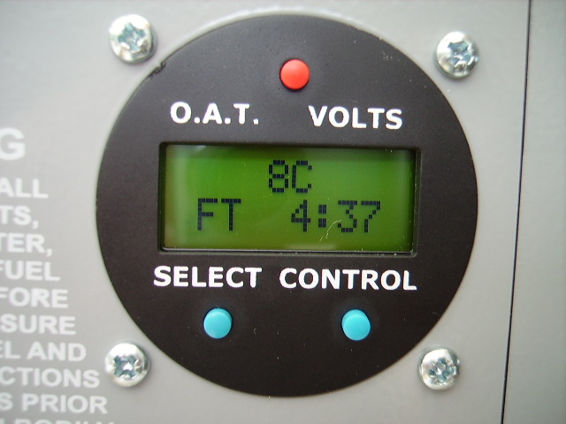
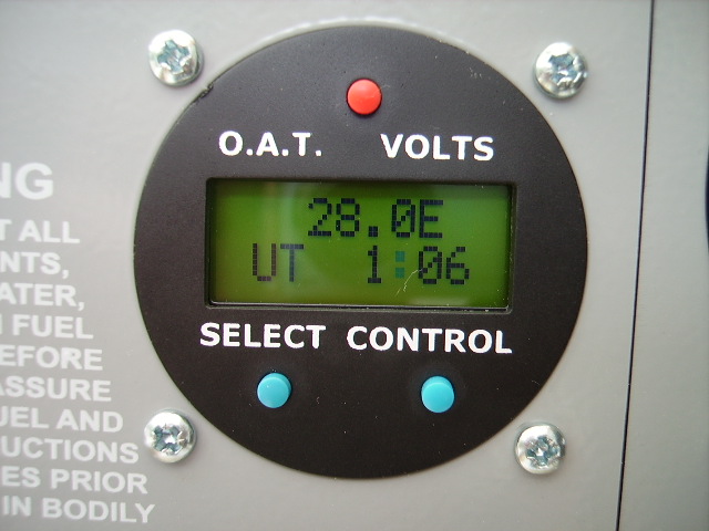
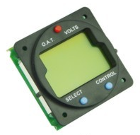
This clock is available from HomeSim based in Germany. It is the most simple of the three clocks shown here. It is basically a standard 2 line by 16 character LCD together display with 3 push button switches and costs approx £100. The clock functionality is provided by another interface board
Simkits Support Documentation
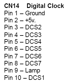
Simkits provide a schematic of the CCU and a pin-out for the clock connector (CN14), but no details of the functionality for each of the pins.
These I/O lines are dedicated as a combination to drive the sub-assembly Digital clock and cannot be controlled by proprietary software, but only via the SDK.
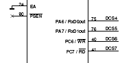
Four of the lines DCS4-7 are connected directly to the CCUs processor chip, which is an AN2131Q.
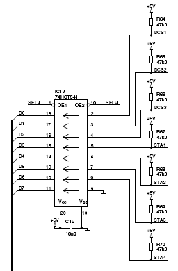
The other 3 lines DCS1-3 are connected through a buffer as inputs.
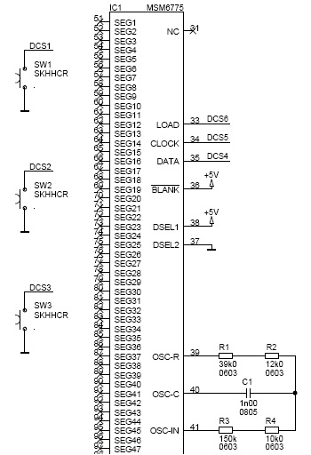
A schematic diagram is available for the Simkits Digital clock that shows DCS1-3 connected to switches, which ground these inputs when activated. DCS4-6 are shown connected to an MSM6775 integrated circuit.
The MSM6775 is an LCD driver from OKI Semiconductors, which is capable of driving an LCD display with up to 400 segments.
From the diagram it can be seen that DCS4 is a data signal, DCS5 is a clock signal, and DCS6 is a Load (synchronisation) signal.
The specification for the MSM6775 defines the operation of the device as follows:
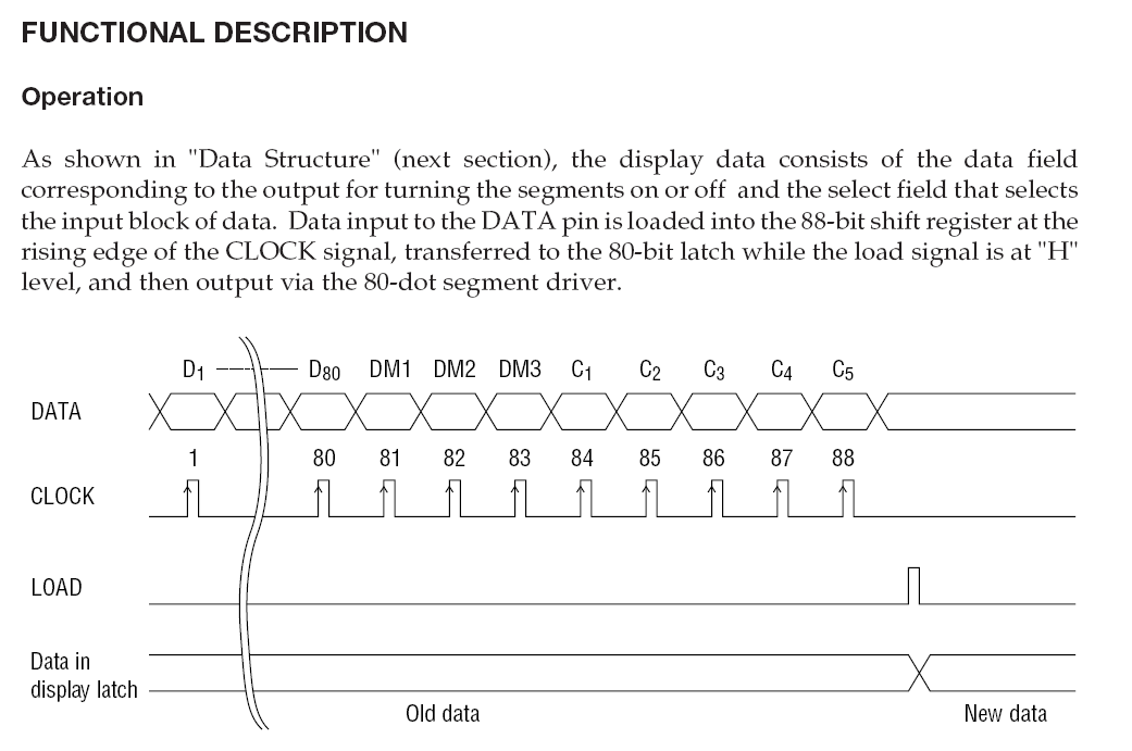
The device functions by receiving 88 bytes of information, followed by a LOAD signal which transfers 80 bytes to the Segments of the LCD display, the remaining 8 bytes of information are used to multiplex the LCD display so that multiple blocks of 80 byte blocks of data can be switched to the Segments of the display. By this mean the number of segments which can be displayed is 80 x number of multiplexing values, in the case of the MSM6775 this is either 3 or 4 or 5 and hence the device is capable of driving either 240 or 320 or 400 segments of an LCD display.
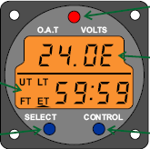
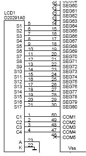
The Simkits clock display is a seven segment LCD unit, capable of displaying four characters plus a decimal point on the first line and 4 characters plus a flashing colon plus four individual enunciator symbols on the second line. The total number of segments to be driven is 8 x 7 (8 off 7 segment characters) + 1 (decimal point) + 2 (separate colon segments) + 4 (enunciators) = 65.
The schematic diagram shows the Simkits LCD display connected to the MSM6775s SEG64 to SEG80 lines i.e. 17 lines. The MSM6775 has been configured, using the DSEL1 and DSEL2 inputs, to work in ¼ mode and the 4 multiplex signals are connected to COM1 to COM4, thus the number of segments displayable on the LCD is 17 x 4 = 68, this exceeds the number of segments calculated above by 3.
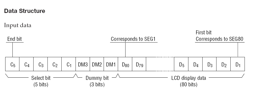
The data format will thus be 4 blocks of 88 bits where the first 17 bits are the segment settings for each multiplexed block and the last 8 bits will be the multiplexing signal.
Interfacing The Display
An oscilloscope was used to probe the lines DCS4-6, the initial findings confirmed that the data was in the form described by the MSM6775 specification.
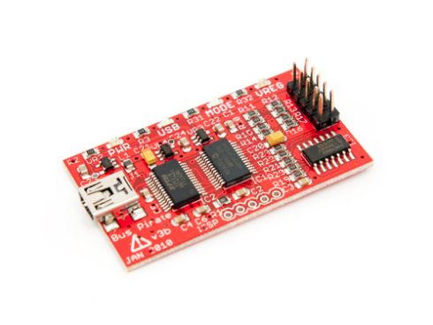
In order to probe the interface further some means of logic analysis would be required. It was decided to purchase a Bus Pirate at a cost of £25. This device can be connected to a PC via a USB interface and can be used to interrogate numerous types of serial interface.
It is even possible to interface this device to a simple logic analyser display.
Bus Pirate Investigation
-
DCS6 this line shows a series of 4 pulses, 9.3uS wide, spaced 494.5uS apart, then gap of 31.4mS before the sequence repeats.
-
DCS5 clock signal, mark is 1.3uS, space is 3.9uS (approx 200kHz). The clock only operates when DCS6 is low. There appear to be 11 blocks of 8 clock pulses between each DCS6 sync pulse, each block of 8 clock pulses is separated by 6.7us.
-
DCS4 data line, logic 1 levels represented by a 2.3us wide pulse.

The sequence between sync pluses is as shown below:

From the above is apparent that there are 4 packets of data, each packet containing 11 off 8 bit words within each frame, as would be expected from the MSM6775 device specification.
Further probing showed that data was only ever present in words 1, 2, 3 as would be expected from the data format derived above of 17 segment bits. Word 11 was always either 00010000 or 00001000 or 00000100 or 00000010, from the MSM6775 this is the multiplexing signal comprised of 3 dummy bits followed by the C5, C4, C3, C2, C1 bits.
Protocol Identification
The data stream is comprised of 4 packets worth of 11 word values, i.e. 44 off 8 bit words, a typical dataset is :
10001011, 11101101, 00000000, 00000000, 00000000, 00000000, 00000000, 00000000, 00000000, 00000000, 00010000,
10011011, 10111111, 10000000, 00000000, 00000000, 00000000, 00000000, 00000000, 00000000, 00000000, 00001000,
10001001, 10110100, 10000000, 00000000, 00000000, 00000000, 00000000, 00000000, 00000000, 00000000, 00000100
01001001, 11101101, 00000000, 00000000, 00000000, 00000000, 00000000, 00000000, 00000000, 00000000, 00000010.
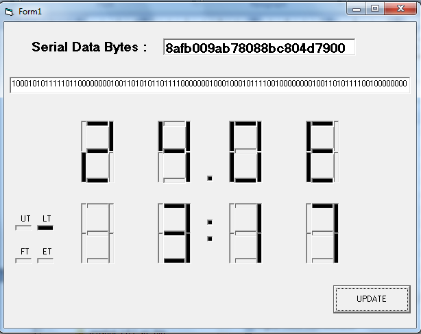
The next task was to determine how the data mapped to the actual segments in the LCD display. In order to map the data to the display it was decided to capture blocks of data for known clock display values. It is possible to set the time values and monitor (although not set) the voltage values from within Microsoft Flight Simulator. Bus Pirate can be configured to sniff (monitor) the serial data line and display the 8 bit words as hexadecimal values. For example the valid words from the data stream shown above would be 8B ED 00 9B BF 80 89 B4 80 49 ED 00 in hexadecimal and would represent 23.4E LT 3:18 displayed on the clock.
Initially an arbitrary numbering scheme for each segment of the character was chosen. Each segment of each character in the display will map to a data bit in the serial data stream. In order to determine if any mapping were present, one character of the display was changed so that only 1 segment of the 7 possible segments changed e.g. changing the hours 10s digit from 8 to 0 would result in segment number 7 being switched off. Another example would be changing from 1 to 7 where segment 1 would be switched on. It was also noted that bits 0 2 of Packet 10, Byte 1 alternated between 1 and 0, this corresponded to the flashing colon character of the hours/minutes display. A spreadsheet was used to record the changes across all 12 of the 8 bit words.
It became apparent that a pattern was emerging and in some cases data could be assumed from previous results. The numbering scheme for the character segments was modified to produce the most logical output. From the above characters a, b, c and d map in a logical sequence, characters g, x, y and z are not so logical with segments 5 and 7 swapped over. The 3rd byte was required because 17 segment signals between the LCD display and the MSM6775 were used.
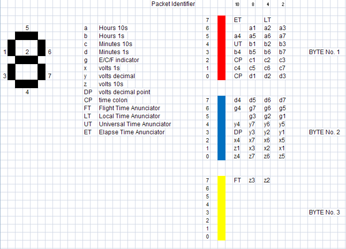
Each 7 segment character in the display is made up from 7 bits of data, split across the four data packets. Using the matrix above, the Hours 10s digit segments are in MSB-LSB order and shown as packet ID bit number: 2-5, 4-5, 8-5, 10-5, 2-6, 4-6, 8-6.
Each 7 segment character will generate a 7 bit data word depending on which character is to be displayed, where an ON segment in the character is a 1 bit and each OFF segment is a 0 bit. The mapping for the characters used in the display and using the matrix shown above is:
|
Character |
ON segements |
Bit Value |
HEX Value |
Map To ASCII |
|
1 |
6,7 |
1100000 |
60 |
31 |
|
2 |
2,3,4,5,6 |
0111110 |
3E |
32 |
|
3 |
2,4,5,6,7 |
1111010 |
7A |
33 |
|
4 |
1,2,6,7 |
1100011 |
63 |
34 |
|
5 |
1,2,4,5,7 |
1011011 |
5B |
35 |
|
6 |
1,2,3,4,5,7 |
1011111 |
5F |
36 |
|
7 |
5,6,7 |
1110000 |
70 |
37 |
|
8 |
1,2,3,4,5,6,7 |
1111111 |
7F |
38 |
|
9 |
1,2,4,5,6,7 |
1111011 |
7B |
39 |
|
0 |
1,2,4,5,6,7 |
1111101 |
7D |
30 |
|
E |
1,2,3,4,5 |
0011111 |
1F |
45 |
|
F |
1,2,3,5 |
0010111 |
17 |
46 |
|
C |
1,3,4,5 |
0011101 |
1D |
43 |
|
SPACE |
|
0000000 |
00 |
20 |
|
- |
2 |
0000010 |
02 |
2D |
In order to verify the results, a simple Visual basic application was produced to allow entry of the 12 hexadecimal values for a captured, known clock display and which would then show the segment representation for the entered values.
A number of data streams were captured and their values checked to verify the bit mapping.
Hardware Implementation
The hardware requirements are:
-
Front Panel
-
Display
-
3 push button switches
-
Interface to decode bit stream
In order to achieve a professional looking result it was decided to purchase the HomeSim clock to fulfil requirements 1-3 rather than try to fabricate a front panel.
Decoder Interface
The requirements are:
-
Read 88 bit stream, which would normally be interfaced to the MSM6775 device.
-
Strip out valid data
-
De-multiplex the packets to seven segment display characters
-
Encode 7 segment display characters to ASCII format
-
Write ASCII format characters to LCD display.
The interface was based on a PIC 16F88 microcontroller. This device has SPI (Serial Peripheral Interface Bus), which although designed for synchronously reading of single 8 bit byte data, can be tricked in to reading multi-byte data streams. This device also has an internal oscillator, capable of running at 8MHz, this will both simplify the design and minimise cost. The interface components are:
-
MicroChip PIC 16F88
-
74HCT04, Hex inverter used to invert the polarity of the switches to match the Simkits CCU, which requires the switches to ground DSC1-3.
-
4K7 resistor
-
100nF capacitor
-
7 pin DIL socket for 74HCT04
-
18 pin DIL socket for 16F88 ( a 28 pin socket was used, in case the 16F88 needed to be swapped for a larger pin count device)
-
Vero-board
-
Connectors
The total cost of the interface was less than £10.
Interface Mapping to the 16F88
The limitations of Port A, where RA5 can only be used as an input pin, restrict the port pins available for the LCD interface. It was decided to use the LCD display in 4bit mode, rather than having to split the interface across Ports A and B and taking in to account that four Port B pins are to be utilised for the SPI interface. Using the LCD display in 4bit mode reduces the interface requirements to 3 control lines and 4 data line and hence Port A can be used, leaving Port B for the serial SPI interface. The 16F88 port allocation is as follows:
|
RA0 |
LCD Display D4 |
|
RA1 |
LCD Display D5 |
|
RA2 |
LCD Display D6 |
|
RA3 |
LCD Display D7 |
|
RA4 |
LCD Display RS |
|
RA6 |
LCD Display RW |
|
RA7 |
LCD Display E |
|
RB1 |
SPI Serial Data In |
|
RB2 |
SPI Serial Data Out |
|
RB4 |
SPI Serial Clock SCK |
|
RB5 |
SPI Select SS |
|
RB3 |
Test LED |
Timing Requirements
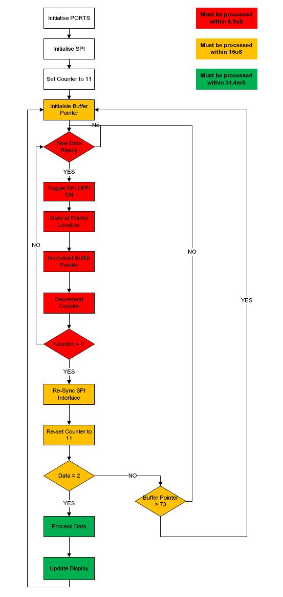
The SPI interface of the 16F88 will be configured to operate in Slave Mode, will be synchronised by the 200KHz clock signal from the CCU2 on pin DCS5 and is dependent on the timing of the serial data stream, which can be considered to operate in four distinct phases:
-
Reception of each of the 8 bits per data byte. This will be controlled by the hardware SPI interface of the 16F88, via the SCK clock signal, running at 200KHz.
-
Reception of the 11 data bytes. The SPI interface expects a single 8bit byte, initiated by the transition on the SS signal. The CCU serial data is generated as 11 bytes while the SS line is held low. The SPI interface can be tricked to receive this multi-byte packet by toggling the SPI interface off and back on between each byte of data. Each data byte is separated by 6.7uS, the 16F88 cycle time per instruction is 0.5uS (at 8MHz) and hence the SPI control, for this section of the code must be achieved in no more than 13 instructions.
-
Reception of the 4 packets in each data frame. The gap between the last byte in a packet and the SS line going back low for the next packet is 16us, hence the SPI control for this section of the code must be no more than 32 instructions.
-
Reception of each frame. The gap between frames is 31.4mS, this time will be used to process the frame of data collected above and update the LCD display.
Timing requirements are such that it will not be possible to
process the received data in real time , hence the data will need
to be stored in a buffer for processing between data frames. In
order to meet the tight timing requirements, the code was developed
in assembler.
The received data will be stored in a buffer area of the 16F88s memory and will be require 44 bytes of memory space. This buffer operates in a similar manner to the MSM6775s data latch, except that it contains the data from 4 latches at once. The buffer will be addressed using an indirect memory access method utilizing a pointer, which will be incremented after each byte is received. The pointer will be re-set after the reception of a byte with a value of 2, indicating the last byte of the last packet within a frame. A separate counter will be used to count the 11 bytes in each packet; this will be re-set at the end of each packet. In order to ensure that a buffer overflow condition does not occur (as a result of a loss of SPI synchronisation), a check will be me at the end of each packet, to ensure that the buffer pointer does not go out of range.
An outline flowchart is shown:
The inner loop is the critical 6.5us timing section and is shown in red. This loop manages the reception of the 11 byte data packet.
The loop surrounding the inner loop is the section which must execute within 16uS and is shown in orange. This loop manages the reception of the 4 packets within a frame.
The outer loop encompasses the relatively long period between the end of one frame and the start of the next, 31.4mS and is shown in green. This loop manages the decoding of the buffered data and the display of the ASCII equivalent characters on the LCD display.
The check that the buffer pointer does not exceed a hexadecimal value of 73 is to ensure that a buffer overflow condition does not occur.
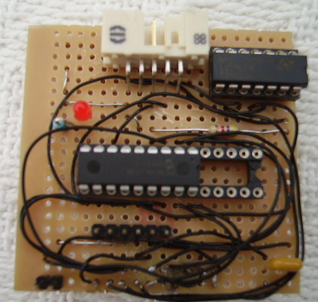
The Working Unit
The prototype interface was constructed on veroboard, the code was generated using MicroLabs MPLAB IDE Ver 8.3 and the 16F88 programmed in situ using a PICKit v2.
The total cost was £120, the interface itself cost £15, and the remainder was for the purchase of the HomeSim digital clock including tax and shipping. The cost could have been reduced dramatically if an LCD display and 3 switches had been purchased separately and mounted on some form of fabricated front plate. The estimated cost of the Simkits CCU clock, including tax and shipping, is £320.
The functionality is exactly the same as the Simkits unit due to the fact that it is being provided by the Simkit CCU2 controller.